
The writer
μLaser is a high value direct laser lithography writer, oriented to universities and research facilities looking to expand their capabilities.
It writes on a photosensitive resist coated surface with a 405nm laser at submicron pixel resolution on big areas. You can write anything from photomasks to research prototypes for basic or applied science, the integrated camera can be used to align the writing with existing features.
We have optimized it for ease of use and simple maintenance, maximizing the use of off-the-shelf parts without sacrificing writing quality or capabilities.
Direct laser lithography
Direct laser lithography greatly reduces costs and execution times in areas such as microfluidics, microelectronics, micromechanics and material science research, by eliminating the dependence of external suppliers for the production of photomasks.
Advantages
High resolution lithography
High resolution lithography
High resolution lithography
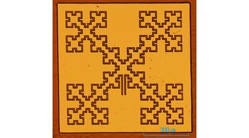
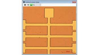
µLaser can get to sub-micron resolution and produce five micron features.
Big writing area
High resolution lithography
High resolution lithography

You can make full size photomasks for production or in-house usage.
User friendly software
High resolution lithography
Change spot sizes easily
µLaser is controlled from an user friendly software on a laptop. It can import GDSII files and PNG images
Change spot sizes easily
Lower price than the competition
Change spot sizes easily
The last lens is an industry standard microscope objective. Replace it to change the spot size!.
We include four microscope objectives.
Use the optics for inspection
Lower price than the competition
Lower price than the competition
Using the confocal yellow illumination and camera you can use the µLaser as a microscope
Lower price than the competition
Lower price than the competition
Lower price than the competition
We have managed to keep the prices low allowing you to have a better lab on a tight budget.
Ultra compact design

microLaser size is only 510x360x455mm and weighs 16kg, making it ideal for use inside of a fume hood or a glove box. Reducing requirements and improving the cleanliness of microfabrication processes.
Options for epoxy photoresist writing

We offer low cost options for direct laser pattering of SU-8/epoxy photoresists for microfluidics and MEMS applications.
Optional extras
Low cost laser for epoxy photoresists
Low cost laser for epoxy photoresists
375nm Laser
Low cost laser for epoxy photoresists
Rotary stage for alignment
Rotary stage for alignment
Software
μLaser is delivered with its control software on a PC. It allows you to import the designs to be written from cells of GDSII files or directly from PNG images.
Everything is done from a user friendly graphical interface that allows you preview the design to write before executing it.
Multiple designs can be combined in a single process, in addition to applying transformations such as rotations, reflections, inversions or scale adjustments to each design.
After defining the design, the included stage control modules and the confocal microscope are used.
With them you set the origin position of the process on the substrate and the focal plane on the photosensitive surface.
Next the process is executed and the design is written on the surface.


Combine it with our mask aligner for maximum capabilities
Our mask aligner, the microAligner, allows for easy fabrication of multilayer devices on a multitude of photoresists, with excellent exposure quality.
The microLaser system, as a complementary tool of the microAligner, offers the possibility for the fabrication of systems, sensors and devices with 3 to 5 µm of minimum feature size. Maskless lithography offers great speed and versatility for the fabrication of new devices and prototyping.
These possibilities make the microLaser and microAligner package the ultimate solution for the fast fabrication and development of multilayered device applications including biomedical, microfluidics and microelectronic devices.
Specs

Mechanics
Size (WxDxH) 510 x 360 x 455 mm
Weight 16kg
Power 110v/220v 400w
XY Stage
Typical writing speed 100-120 mm/s
Maximum area 100x92 mm^2
Minimum area There isn’t a minimum area
Unidirectional positioning step X = 0.16 µm, Y = 1.00 µm
Multi layer aligning accuracy 5-10 µm (Optional rotary stage for easier aligning)
Mechanical noise on the slow X axis ≈ 150nm RMS
Mechanical noise on the fast Y axis ≈ 50nm RMS
Realistic minimum feature size 2-4µm depending on the feature (see pictures below for examples)
Software
Supported formats PNG,GDSII
In-software transformations Rotation, Reflection, Inversion, Rescaling, Add border
-Multiple designs from different files can be written in one process
-Tilted/warped substrate compensation via 3-point linear or 4-point bilinear focus measurement
-Mesh type calibration for full-bed curvature compensation
Optics
-Laser wavelength: 405nm (optional 375nm)
-Confocal microscope for laser focusing, aligning and inspection
-Secondary independent yellow illumination
-Laser spot size can be changed using industry standard microscope objectives
Raster step of included objectives:
-Fine: 0.8 µm
-Medium fine 0.96 µm
-Medium: 2 µm
-Coarse: 5 µm
Effective writing speed of included objectives on big areas (unidirectional writing):
-Fine: 2.0 mm^2/min
-Medium fine 2.5 mm^2/min
-Medium: 4.25 mm^2/min
-Coarse: 12.6 mm^2/min
Speed doubles in bidirectional writing mode.